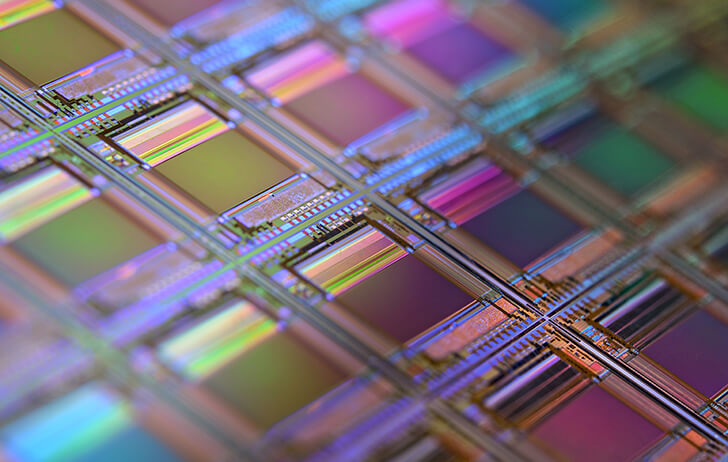
Canon has partnered with Tokyo Electron and Screen Semiconductor Solutions to develop advanced chipmaking production technology with support from the Japanese government according to a report by Nikkei Asia.
The $386mil USD funding from the Japanese government is through the National Institute of Advanced Industrial Science and Technology, along with the Ministry of Economy, Trade and Industry (METI).
Japans semiconductor production industry has lost ground in recent years to Taiwanese chipmakers and companies like Intel.
The goal is to develop and implement a 2-nanometer or smaller process for chips by the mid-2020s.
Some of our articles may include affiliate links. If you purchase through these links, we may earn an affiliate commission at no extra cost to you.


If they think they can get results at 2nm for that price, I'd be willing to bet that they can pull it off within that price, with maybe some extra for unforseen issues. If Canon happens to come out with even better sensors & processors because of it, then we'll also be the beneficiaries of it. :)
Now, if only the US had the foresight to do something like this ...
When I lived and worked in Japan (late 90’s) Canon and Nikon and even ultratech all had fair share. NEC was #2 in semiconductor revenue.
The industry has changed.
Latest immersion scanners / i193 it is mostly ASML ...with Zeiss lenses. Strong manufacturing engineering control makes them better than Canon or Nikon. For the latest technology / EUV, the 400M$ is noise....Intel alone invested 4B$ in ASML....each tool is >100M$.
Sony, Canon and to some extend Kioxia are just small niche players...this 400M$ won’t change that...
TWINSCAN NXT:2000i
bit like Sony‘s camera’s
I may even buy a body just for that!