Sony CorporationSony Semiconductor Solutions Corporation Tokyo, Japan – Sony Corporation today announced that it has developed a 1.46 effective megapixel back-illuminated CMOS image sensor equipped with a Global Shutter function*¹. The newly developed pixel-parallel analog-to-digital converters provide the function to instantly convert the analog signal from all pixels, simultaneously exposed, to a digital signal in parallel. This new technology was announced at the International Solid-State Circuits Conference (ISSCC) on February 11, 2018 in San Francisco in the United States.
CMOS image sensors using the conventional column A/D conversion method*2 read out the photoelectrically converted analog signals from pixels row by row, which results in image distortion (focal plane distortion) caused by the time shift due to the row-by-row readout.
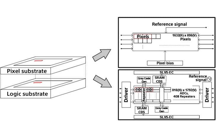
The new Sony sensor comes with newly developed low-current, compact A/D converters positioned beneath each pixel. These A/D converters instantly convert the analog signal from all the simultaneously exposed pixels in parallel to a digital signal to temporarily store it in digital memory. This architecture eliminates focal plane distortion due to readout time shift, making it possible to provide a Global Shutter function*¹, an industry-first for a high-sensitivity back-illuminated CMOS sensor with pixel-parallel A/D Converter with more than one megapixel*³.

The inclusion of nearly 1,000 times as many A/D converters compared to the traditional column A/D conversion method*² means an increased demand for current. Sony addressed this issue by developing a compact 14-bit A/D converter which boasts the industry's best performance*4 in low-current operation.
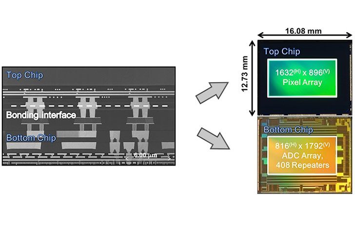
Both the A/D converter and digital memory spaces are secured in a stacked configuration with these elements integrated into the bottom chip. The connection between each pixel on the top chip uses Cu-Cu (copper-copper) connection*5, a technology that Sony put into mass production as a world-first in January 2016.
In addition, a newly developed data transfer mechanism is implemented into the sensor to enable the high-speed massively parallel readout data required for the A/D conversion process.
*1:A function that alleviates the image distortion (focal plane distortion) specific to CMOS image sensors that read pixel signals row by row.*2:Method where the A/D converter is provided for each vertical row of pixels in a parallel configuration.*3:As of announcement on February 13, 2018.*4:As of announcement on February 13, 2018. FoM (Figure of Merit): 0.24e-?nJ/step. (power consumption x noise) / {no. of pixels x frame speed x 2^(ADC resolution)}.*5:Technology that provides electrical continuity via connected Cu (copper) pads when stacking the back-illuminated CMOS image sensor section (top chip) and logic circuits (bottom chip). Compared with through-silicon via (TSV) wiring, where the connection is achieved by penetrating electrodes around the circumference of the pixel area, this method gives more freedom in design, improves productivity, allows for a more compact size, and increases performance. Sony announced this technology in December 2016 at the International Electron Devices Meeting (IEDM) in San Francisco.
Main Features
Global Shutter function*1 achieved in a high-sensitivity back-illuminated CMOS image sensor by using the following key technologies:
Low-current, compact pixel-parallel A/D converter
In order to curtail power consumption, the new converter uses comparators that operate with subthreshold currents, resulting in the industry's best-performing*4, low current, compact 14-bit A/D converter. This overcomes the issue of the increased demand for current due to the inclusion of nearly 1,000 times as many A/D converters in comparison with the traditional column A/D conversion method*2.
Cu-Cu (copper-copper) connection*5
To achieve the parallel A/D conversion for all pixels, Sony has developed a technology which makes it possible to include approximately three million Cu-Cu (copper-copper) connections*5 in one sensor. The Cu-Cu connection provides electrical continuity between the pixel and logic substrate, while securing space for implementing as many as 1.46 million A/D converters, the same number as the effective megapixels, as well as the digital memory.
High-speed data transfer construction
Sony has developed a new readout circuit to support the massively parallel digital signal transfer required in the A/D conversion process using 1.46 million A/D converters, making it possible to read and write all the pixel signals at high speed.

