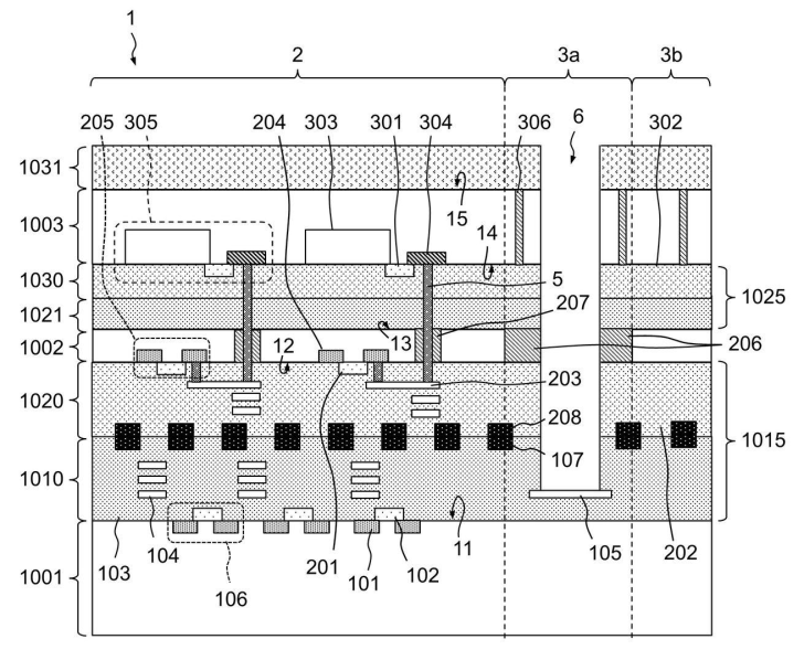
One of the most hotly patented and contested areas of sensor patent space is how stacked substrates talk to each other. Before Canon released its first stacked sensor in the R3, I had lost count of how many stacked sensor patents dealt with the interconnects between 2 substrates. Usually, the more interconnects between the subtracts the more complex and costly it is. Each pixel usually “talks” to the second substrate because that's where all the logic and the ADC circuitry reside. So there's a fair amount of connections between the top and bottom substrate.
This is one of the first patent applications (2024-011954) I've seen where Canon takes it all a step further and introduces a third layer. I've seen conceptual patent applications with 3 layers, but none with a method of manufacturing. I may have missed some as these are easy to glance over and miss when you are looking through all the patents, but certainly, this is a step forward in Canon expanding to a 3 layer-stacked sensor design. Patents that detail the method of manufacturing are more about the “how to make it” cost-effectively and efficiently.
The more patents we see with these kinds of sensor designs the more likely Canon will take the next step in sensor manufacturing. Sony, of course, is already there with 3 (and I think 4 more) layers – as atypically they use the 3rd layer for memory.
Canon starts off the patent application with;
An object of the present invention is to provide a technique advantageous for improving the characteristics of a semiconductor device in which a plurality of semiconductor layers are stacked.
And then it quickly gets Japanese machine language translation obscure from there.

Even though this is shown above, I'll briefly break down this diagram so it's good to have it right here with us in the document for ease of following along. When I first looked at this diagram I got it all confused. This diagram is more for a description of the sections and is not to scale. Sections of interest are made larger so that Canon can explain it more clearly in the patent application.
- 1031 is the section of the sensor that may have light shielding (for the masked pixels), color filter array, and microlenses. Basically in the drawing, it's a catch-all for everything that is attached to the top surface of the sensor.
- 1003 – that's the first substrate of the sensor.
- 1030 and 1021 are insulating layers between substrates.
- 1002 is the second substrate.
- 1020 identifies the structures formed on top of the 1002 substrate.
- 1010 identifies the structures formed on top of the 1001 substrate.
- 1001 is the third substrate.
- 303 and 305 – These are the photodiodes represented in the diagram.
- 304 is the floating diffusion layer of the photodiode
- 5 is a plug electrode connecting substrates 1003 and 1001.
- 6 is an opening that exposes pad 105 in the bottom substrate
- 106, 205 is the transistor switch for the photodiode
- 104 and 203 identify wiring in the associated substrate layers.
- 208 and 107 are bonding pads that allow for communication between the second layer and third layer.
Hopefully, the more patent applications we see with Canon exploring this technology will signal Canon taking the next step in sensor fabrication. They pleasantly surprised us with the R3 sensor, so anything is certainly possible. Keep in mind this is just research. this in no way means we are going to see this technology on an R1, or a Canon camera coming out soon. But it shows what Canon is researching and potentially developing for the future.
Source: Japan Patent Application 2024-011954


thanks for the catch