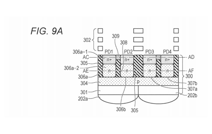
Canon continues to work on new sensor designs based on the patents we've seen over the last year or so. This patent covers a lot of things, most notably a backside illuminated sensor, or more commonly known as BSI.

Canon News writes:  (USPTO 20190035827

Much has been made over Sony's BSI (back side illuminated) sensors, and I'm sure Canon is certainly researching making their own.  BSI sensors have efficiency gains not found in normal sensors.  They are also much better in mirrorless cameras because the light doesn't have to penetrate as deep into the sensor, and mirrorless cameras have a higher angle of incidence of light hitting the sensor near the corners.

We expect some big gains in Canon sensor technology once the next generation of sensors makes it to consumer products.

Some of our articles may include affiliate links. If you purchase through these links, we may earn an affiliate commission at no extra cost to you.

Go to discussion...

Share.

40 comments

  1. Finally! I was hoping Canon would eventually start looking long and hard at backside illuminated designs. And I'm quite happy they're designing it around DPAF sensor architecture. This will have a huge benefit for low-light performance on high MP sensors.
  2. Finally! I was hoping Canon would eventually start looking long and hard at backside illuminated designs. And I'm quite happy they're designing it around DPAF sensor architecture. This will have a huge benefit for low-light performance on high MP sensors.

    Has that low light benefit been demonstrated anywhere? It seems that gapless microlenses render it a bit of a moot point. BSI is required, as far as I know, for stacked architecture, which will help alleviate bandwidth limitations as pixel counts increase and real time image analysis requirements grow. To me that’s the primary advantage.
  3. Has that low light benefit been demonstrated anywhere? It seems that gapless microlenses render it a bit of a moot point. BSI is required, as far as I know, for stacked architecture, which will help alleviate bandwidth limitations as pixel counts increase and real time image analysis requirements grow. To me that’s the primary advantage.

    Yes, gapless microlenses have helped improve the sensitivity of photodiodes, but the big benefit of BSI is the removal of the transistors from the surface area. That way you maximize the area and volume of the light sensitive region of the photodiode. It provides a bit of a boost to full-well capacity in most cases. But I've heard there's a trade-off in terms of noise performance. What BSI sensor designs tend to gain in light sensitivity and improved photon (shot) noise performance, they end up losing a bit of read noise performance because the transistors are embedded deeper in the silicon where more dark current is generated. And yes, the potential of stacked sensor designs is perhaps the most significant advantage to be had with BSI architectures.
  4. Can someone more experienced chime in and say if it possible that we see this technology in the next cmaeras, like 7d iii?

    How has it been in the past? Do those patents get quickly implemented in new products?
  5. Can someone more experienced chime in and say if it possible that we see this technology in the next cmaeras, like 7d iii?

    How has it been in the past? Do those patents get quickly implemented in new products?

    Canon's been looking at BSI for a while now, including BSI stacked patents. We have found quite a few in the last year or so.

    In theory, Canon could implement quickly, it really depends on the complexity of how you actually create a BSI sensor - it's a little tricky. Stacked sensors which Canon has done a ton of patent work on, may be easier to implement and provide nearly the same benefits as BSI, because with a stacked sensor BSI is less important because the transistors and wiring mostly exist in the secondary layer and not the photodiode layer.

    Canon's been looking at a ton of different things, from stacked sensors, curved sensors, even curved stacked sensors (a real unicorn), BSI sensors .. you name it Canon's been researching it.

    just doing a quick search on our site, i see 17 stacked sensor patents, 5 BSI patents, and 5 curved patents. this in a little over a year since we've been online.
  6. Yes, gapless microlenses have helped improve the sensitivity of photodiodes, but the big benefit of BSI is the removal of the transistors from the surface area. That way you maximize the area and volume of the light sensitive region of the photodiode. It provides a bit of a boost to full-well capacity in most cases. But I've heard there's a trade-off in terms of noise performance. What BSI sensor designs tend to gain in light sensitivity and improved photon (shot) noise performance, they end up losing a bit of read noise performance because the transistors are embedded deeper in the silicon where more dark current is generated. And yes, the potential of stacked sensor designs is perhaps the most significant advantage to be had with BSI architectures.
    But have those gains been demonstrated, even in a lab? I’ve looked for quantitative apples to apples comparisons of BSI to FSI, and haven’t found anything (not that I’ve looked particularly hard).
  7. The patent is not about BSI, but a manufacturing method for the Pixels in a DPAF or Quad Pixel or even other split multi pixel sensor. It shows different examples, and while examples 1- thr 8 are conventional Front side wiring, it shows in example 9 how BSI sensors would make use of the manufacturing method.

    The issue they are trying to solve is isolation performance between a plurality of photoelectric conversion portions(dual pixels or quad pixels for example) where some wavelengths of light are not isolated as well as desired.

    So, yes, it mentions BSI in passing, but its not about BSI at all.
  8. I remember there is a collaboration between Canon & Sony quite some times ago as both of them agreed to ex-change their technology to photography equipment.

    Canon is exchanging their DPAF with Sony sensor technology. Of course both of them won’t handouts everything they have.

    Thus we can see the great improvement of Sony AF and now Canon is about to improve their sensor performance.

    Good for the consumer.

    Thanks.
  9. I remember there is a collaboration between Canon & Sony quite some times ago as both of them agreed to ex-change their technology to photography equipment.

    Canon is exchanging their DPAF with Sony sensor technology. Of course both of them won’t handouts everything they have.

    Thus we can see the great improvement of Sony AF and now Canon is about to improve their sensor performance.

    Good for the consumer.

    Thanks.

    There was some speculation that Canon and Samsung had some sharing. Indeed Samsung has DPAF products. Sony does not.
  10. "We expect some big gains in Canon sensor technology once the next generation of sensors makes it to consumer products. "
    Might this just be for their commercial focus on monitoring systems.
    With Focusing down to -6eV (with the right lens) then sensors do need to work harder.
  11. But have those gains been demonstrated, even in a lab? I’ve looked for quantitative apples to apples comparisons of BSI to FSI, and haven’t found anything (not that I’ve looked particularly hard).

    IEEE is probably the best resource for looking into differences between CMOS architecture for active pixel sensors. This whitepaper in particular is a brief overview of differences in fill-factor and peak QE between FSI and BSI designs (but there are plenty more): https://ieeexplore.ieee.org/stamp/stamp.jsp?arnumber=8334288

    In practice the gains of BSI are realized with very small pixel sizes - usually between 1-3 micrometers per side. That's why almost every smartphone sensor (1/2.3" or smaller) and most premium compacts have all adopted BSI designs.
  12. IEEE is probably the best resource for looking into differences between CMOS architecture for active pixel sensors. This whitepaper in particular is a brief overview of differences in fill-factor and peak QE between FSI and BSI designs (but there are plenty more): https://ieeexplore.ieee.org/stamp/stamp.jsp?arnumber=8334288

    In practice the gains of BSI are realized with very small pixel sizes - usually between 1-3 micrometers per side. That's why almost every smartphone sensor (1/2.3" or smaller) and most premium compacts have all adopted BSI designs.
    Youre repeating that old information I just posted about, having not seen your post first. Sensor manufacturers are now using this on larger sensors, so thoughts about this must have changed.
  13. It wasn’t all that long ago that we were being told that this is only useful for small sensors. What’s changed?
    I think the number of steps required in each layer that laid down have been greatly reduced. I think the only reason why it was only used in phone sensors before was that it was only economical if you were making thousands of sensors per wafer. (for example at $15 per phone sensor you'd be looking at 10,000+ as a full frame sensor). The sensor used to be one of the most expensive parts of a top end phone. These days they are cheap enough they can put 6-7 on them phone.
  14. This is good news but Canon needs to move quickly. Given the CEO's gloom market forecast, is Canon truly devoted to the task?

    Looking at Canon core business and competencies, the obvious answer is yes. Looking at the number of patents... that is, a proxy for research, the answer would also be yes.

Leave a comment

Please log in to your forum account to comment