Is Vistilen the Next Third-Party RF Lens Manufacturer?
- Third Party Manufacturers
- 19 Replies
Who cares. Just get those lenses out there. Meike optics are great, as is their AF (on Sony, at least).
Upvote
0
I would guess that it is a combination of Vista + Lens. The Chinese like having syllables from western words in their naming.Vistilen? Why not Vilisten, Vinistel, Vilistine? Who names them that way and why?
Agree it's not as simple as just ramping up production."Ported" and being able to actually make enough are different things. A lens like the 135 f/1.4 would be a very difficult lens to make within tight tolerances. Sigma made nothing worth owning for most of the EF days. When they did start making things that were sort of nice there were already 100+ million EF lenses. Having worked directly with Gentec, I know how few lenses they sold in the grand scheme in at least one market (maybe 2). It was peanuts.
Demand increasing 30% is great, now you have to scale everything else 30%. There's a point in lots of businesses where the next step costs exponentially more than the previous one.
Take a company like Leica (yes, they do it different). They make 40 cameras a day. Major products usually take about a year to meet the demand. How much would it cost them to increase production to 60 a day? A boatload. Sigma is closer to Leica than they are to Canon. Leica's revenue is actually higher than Sigma's.
or faster lenses which are more expensive, bigger, heavier and have less DOF.you need a bigger sensor to collect more light

That's the SLR era lens. It was excellent but is huge, heavy, and the AF is very slow by today's standards.
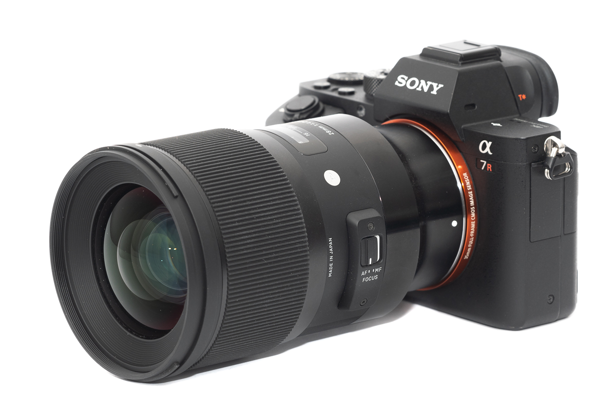
Review: Sigma 28mm 1.4 Art - phillipreeve.net
The Sigma 28mm 1.4 Art is the only fast 28mm fullframe lens for Sony E-mount with reliable Autofocus, but is it alsophillipreeve.net
Oh look, it's the #1 member of the Cult of Canon! He's continuing to drink the Flavor Aid, I'm so surprised. /sHe was talking about production capacity for cameras and lenses, which is very relevant to the topic at hand. Market cap…isn’t. But thanks for trying, at least you’re spot on about not getting the point.
To reiterate: If you want less noise at high ISO (i.e., better actual image quality), you need a bigger sensor to collect more light. It's really that simple, despite your amply and thoroughly demonstrated unwillingness or inability to accept that.[...]
At the end of the day, clarity—actual image quality—is what most photographers are aiming for.
I don't have a camera that hasn't been launched yet. R1 with the RF 85/1.2L DS.This thread began discussing the R7 Mark II. The conversation lately seems to be more theoretical and more general in nature.
Was your cat's eye example taken with an R7 or R7 Mark II?

I understand the point about shot noise dominating at higher ISOs and that total light collection is a primary driver of overall noise—that’s well established.Lots of misunderstandings and irrelevancies there...and I won't address most of them.
If crop your images to a few hundred pixels, then that might even matter. For example, it might make a difference in this picture of one of my cats.
View attachment 228732
But...that's not really much of a picture now, is it?
As I mentioned previously, at the light levels where those ISOs are used shot noise dominates and read noise is essentially irrelevant. All of the 'improvements' that you think are meaningful (bigger pixels, BSI, per-pixel S/N, etc.) affect read noise, albeit in a functionally insignificant way. Shot noise is dependent on the amount of light being collected by the sensor, meaning all of your arguments about this issue are irrelevant.
If you want less noise at high ISO, you need a bigger sensor to collect more light. It's really that simple, despite your unwillingness or inability to accept that.
While you're hoping for that meaningful improvement in high ISO noise performance in the R7II, you should also hope for unicorn rides and for Canon to set the price for the R7II at $14. Those are all at just about the same level of likelihood, the only difference being the first one is not going to happen because of physics while the last two are just silly fantasies.
Note that we are discussing the R7II, not cameras from well over a decade ago. Having said that, even with current sensors (not just Canon) there is a shift in the amount of noise at the ISO values where second (and sometimes third) stage amplifiers come into play.
Technically correct, practically irrelevant. Even at base ISO...what is base ISO? Setting a camera to ISO 100 (or whatever its lowest non-expanded ISO setting is) does not mean that's the base ISO. Differences in real base ISO between one camera model and the next also fall into that 'practically irrelevant' category. Important to pedants and measurebators, not to photographers.
Sure, you can stand up and argue that when set to ISO 400, one APS-C camera has the image noise of ISO 412 and another has the noise of ISO 397. BFD. For an APS-C camera set to ISO 400, a full frame camera set to ISO 1000 would have same the image noise, and that's a meaningful difference.
Note that we are discussing the R7II, not cameras from well over a decade ago. Having said that, even with current sensors (not just Canon) there is a shift in the amount of noise at the ISO values where second (and sometimes third) stage amplifiers come into play.For most of Canon's FF and APS-C cameras in the late 2000s and early 2010s, ISO 125 was noisier than ISO 800! I saw other similar tests from other websites which are no longer still up.
Sadly no 28/1.4 yet

 phillipreeve.net
Technically correct, practically irrelevant. Even at base ISO...what is base ISO? Setting a camera to ISO 100 (or whatever its lowest non-expanded ISO setting is) does not mean that's the base ISO. Differences in real base ISO between one camera model and the next also fall into that 'practically irrelevant' category. Important to pedants and measurebators, not to photographers.
Sure, you can stand up and argue that when set to ISO 400, one APS-C camera has the image noise of ISO 412 and another has the noise of ISO 397. BFD. For an APS-C camera set to ISO 400, a full frame camera set to ISO 1000 would have same the image noise, and that's a meaningful difference.
If crop your images to a few hundred pixels, then that might even matter. For example, it might make a difference in this picture of one of my cats.At the same time, I don’t think it’s accurate to say pixel size is irrelevant. On a fixed sensor size, increasing resolution reduces pixel area, which affects per-pixel signal-to-noise. While normalization can reduce those differences when images are resized, in real-world use—especially at high ISO—those factors can still influence how noise presents in the actual image.

As I mentioned previously, at the light levels where those ISOs are used shot noise dominates and read noise is essentially irrelevant. All of the 'improvements' that you think are meaningful (bigger pixels, BSI, per-pixel S/N, etc.) affect read noise, albeit in a functionally insignificant way. Shot noise is dependent on the amount of light being collected by the sensor, meaning all of your arguments about this issue are irrelevant.My concern is more about how these cameras are actually used. For action and wildlife photography, I’m often shooting at ISO 3200–6400+ to maintain shutter speeds around 1/1000, and I’m not downsampling to evaluate noise—I’m looking at the image at native resolution or cropping, which is very common in birding. In that context, how noise presents in the actual file matters, not just how it behaves after normalization.
While you're hoping for that meaningful improvement in high ISO noise performance in the R7II, you should also hope for unicorn rides and for Canon to set the price for the R7II at $14. Those are all at just about the same level of likelihood, the only difference being the first one is not going to happen because of physics while the last two are just silly fantasies.As an action photographer, I’m really hoping the Canon EOS R7 Mark II does deliver a meaningful improvement in noise performance.
Technically correct, practically irrelevant. Even at base ISO...what is base ISO? Setting a camera to ISO 100 (or whatever its lowest non-expanded ISO setting is) does not mean that's the base ISO. Differences in real base ISO between one camera model and the next also fall into that 'practically irrelevant' category. Important to pedants and measurebators, not to photographers.It does affect full well capacity, though. This means a change in analog amplification levels to avoid blowing out highlights, which means other sensels with very little light striking them are also amplified less, which puts them closer to the read noise floor (but not Poisson distribution noise, which is reduced proportional to the area of each sensel). So this is mostly a thing for base ISO. Is it near the difference of an APS-C sensor compared to a FF sensor? No, it is not. But the difference is still there. The same with BSI vs non-BSI sensors. The smaller each sensel is, the higher percentage of that sensel is blocked from incoming light by the circuitry. Gapless lenses in front of the sensor help to refract more of the light towards the parts of the sensel where there is no circuitry, but they're not precise enough to completely redirect all light to areas of each sensel with no circuitry blocking it. Dual Pixel AF sensors have twice as much circuitry as sensors with the same "effective" resolution which are not Dual Pixel AF sensors. Again, is it near as significant with sensels in the 3-4µm neighborhood as with phone sensels in the sub 1µm range? No, but it's still there.
Now the problem I have with all the "rumours" or speculation is that it was suggested strongly that this MII was targeted for action shooters. If that is the case (and I now question if that rumour was true), then they should not have increased pixel density (it wasn't necessary) at the cost of the same or worse signal to noise in the camera.
