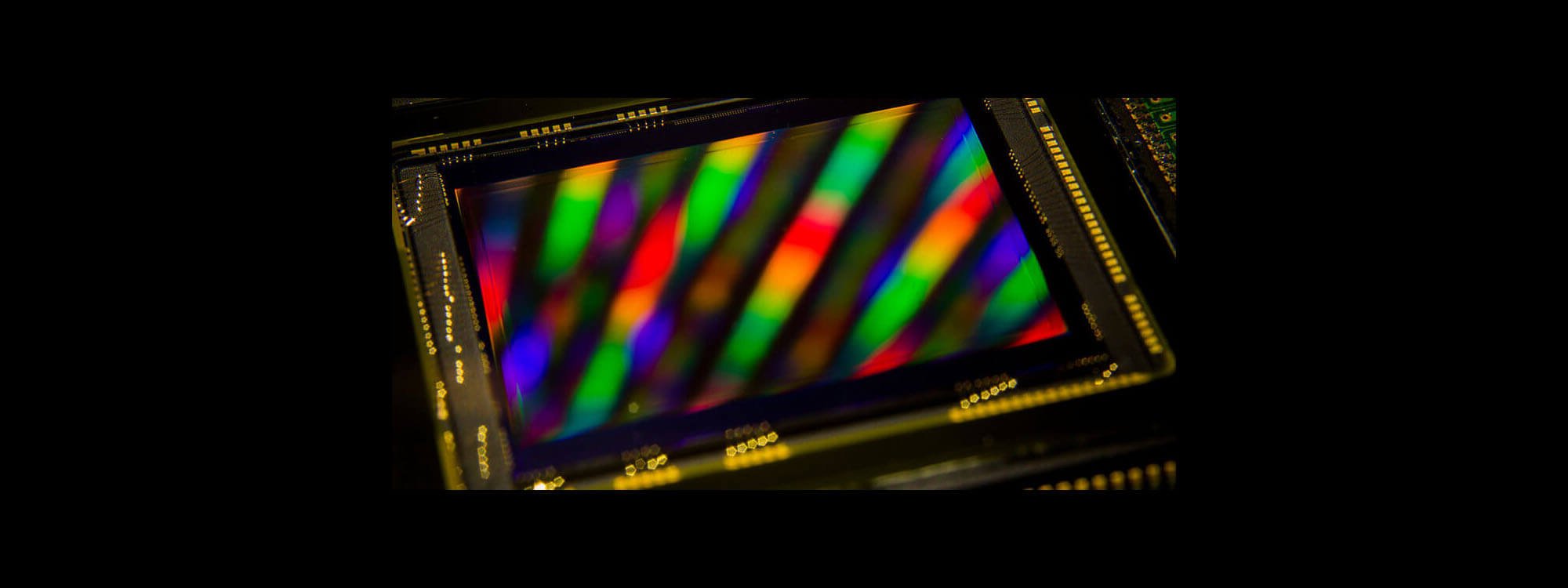
Canon Unveils New Global Shutter Sensor for Third-Party Use
Canon has placed the LI5070SA sensor on its website for third-party sales.…
Canon Patent Application: Hybrid IR/Color sensor to improve Image Quality
We will be releasing an upcoming series of articles on infrared photography…

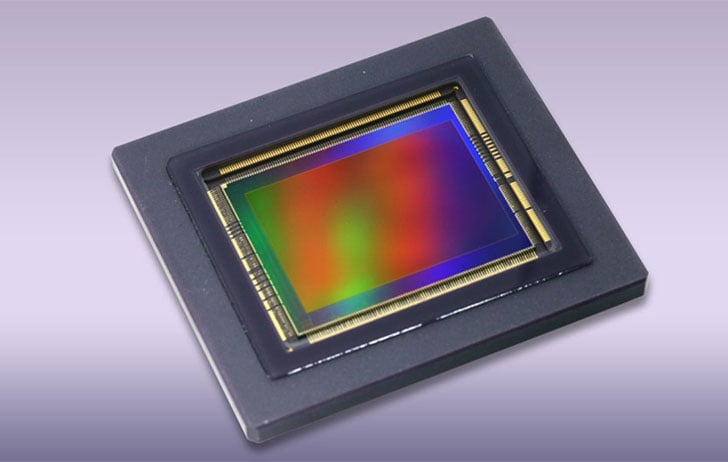
Canon Patent Application: Triple-layer High Speed Stacked Sensor
In this patent application (2024-019961) Canon shows off a high-speed stacked sensor…
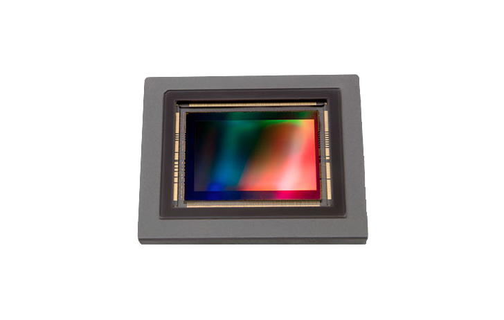
Canon Patent Applications for High Dynamic Range Sensors
A couple of patent applications caught my eye over the last week…

Canon is looking to partner with a smartphone manufacturer
A few weeks ago reports came out that Canon was looking for…

Has Canon developed a new 21mp sensor for the Canon EOS R system? [CR1]
Canon Watch is reporting that Canon has developed a new 21mp full-frame…
Canon U.S.A. Announces New 120 MP Ultra-High Resolution and 2.7 MP Ultra-High Sensitivity CMOS Sensors
MELVILLE, NY, June 20, 2019 – As image sensors are a driving force…
Canon Announces Development of New CMOS Sensor with High Dynamic Range and Ability to Capture Images Under Harsh Conditions
MELVILLE, NY, June 20, 2019 – The high demands of complex lighting…
A leaked document suggests that Canon has a 63mp full frame image sensor in the works.
*Update* After speaking with a couple of people, it turns out that…
Is the term ISO “totally fake”?
Tony Northrup has posted a video discussing the exposure term ISO and…

Off Brand: Sony 36mp full frame sensor capable of 4K at 480fps leaks
It looks like Sony has no intention of resting on the laurels…
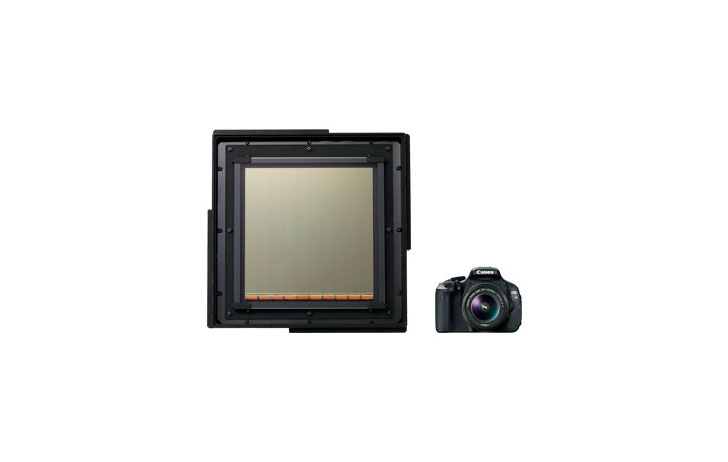
The World’s Largest Ultrahigh-Sensitivity CMOS Image Sensor
Canon has posted an article about what they claim is "The World's…