Canon has released a couple of stacked sensor patent applications this week dealing with various issues surrounding the manufacturing or use of stacked sensors.
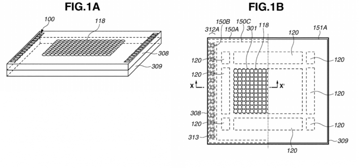
In US Patent Application 2018-0233523, they discuss sealing to form a moisture proof barrier thus protecting the internal elements from water,etc. This is another highly detailed sensor patent, with methods of manufacturing included, indicating that Canon is quite a ways into this research.
According to an aspect of the present invention, a solid-state imaging apparatus includes a plurality of pixels each of which includes a photoelectric conversion unit and a readout circuit configured to process a signal generated by the photoelectric conversion unit or configured to read the signal, and a peripheral circuit configured to read signals from the plurality of pixels. The plurality of photoelectric conversion units is disposed in a first member, and at least a part of the readout circuit and the peripheral circuit are disposed in a second member. The first member and the second member are bonded in such a way that a signal from the photoelectric conversion unit can be received by the readout circuit disposed in the second member. The solid-state imaging apparatus includes a sealing portion configured to reduce water invasion from an outside region of the solid-state imaging apparatus into the plurality of pixels and the peripheral circuit, wherein the sealing portion includes a first sealing portion disposed in the first member and a second sealing portion disposed in the second member, and a part of the first sealing portion is in contact with a part of the second sealing portion.
Further, in US Patent Application 2018-0234605 they discuss using the second substrate to control exposure, thus having more flexibility including having sensors capable of extremely fast speeds, for example, up to 1000 fps. The main goal is to offload the burden of micro aperture and gain adjustments as exposure changes and have that handled all by the sensor in a far more efficient manner.
The present invention provides an imaging element which controls exposure and an imaging apparatus which can reduce an amount of an exposure control process of an arithmetic processing unit using the imaging element.
According to an aspect of the present invention, an image processing apparatus that outputs an image signal acquired by an imaging unit which has a plurality of pixel units is provided that includes a gain unit that sets gain with respect to an output signal of the imaging unit; a control unit that controls an accumulation time of the pixel units; and an arithmetic operation unit that receives a target luminance value and exposure control information, calculates the gain or the accumulation time by detecting a luminance value using an image signal read from the pixel units, and causes the gain unit or the control unit to perform exposure control of the imaging unit.
According to the present invention, an amount of an exposure control process of an arithmetic processing unit can be reduced by using an imaging element which controls exposure.


A 1D X III with a 1,000FPS e-shutter sounds like a good answer to the competition. I'll take two please.
A 2nd method is to place the circuitry on the rear of the sensor wafer, thats referred to as BSI or back side illumination. It brings lots of problems and is difficult.
So, the circuitry can be placed on a separate wafer which is stacked with the sensor wafer and has connections to the photodiodes. This allows for more complex circuitry, and a large ground plane. That large ground plane allows for much faster frame rates because they are greatly limited by the grounding path and noise generated from the switching. A whole new set of issues and expense comes into play with stacked sensors, but they solve problems, so expect everyone to use them once they can make them work.
Right now, Sony makes stacked sensors and pretty much has the field to themselves. It was not easy for them to do it, so its a potential benefit.
We do not know when or if Canon will be able to produce them, they usually are implemented for small sensors first. Canon has been using Sony 1 inch sensors that are BSI, and might like to make their own stacked sensors.
https://www.3dincites.com/2014/09/future-image-sensors-chip-stacking/
The encouraging news for all of this is the fact that they are throwing out so many patents for manufacturing techniques. Canon has always been patent happy, but when you see patents for manufacturing processes it means they are working out the kinks for mass production usually. It doesn't mean any one method is being used because it's patented, but it does mean that what the type of chip the patents pertain to is something actively being pursued and most likely produced.
<iframe width="560" height="315" src="
https://fuse.wikichip.org/news/763/iedm-2017-sonys-3-layer-stacked-cmos-image-sensor-technology/
Sigma's Foveon is a stacked RGB standard CMOS. Standard as in it functions the same way a Bayer CFA does in terms of pixel-level signal amplification and on-sensor ADC. This patent pertains to a secondary substrate layer for faster processing like the Sony EXMOR.